PHOTOCHUCKS
You want to upgrade your tool with the best possible photochuck available on the market?
Lithotools are the most capital-intensive tools in a semiconductor fab. Next to the optics, the Chuck itself can influence the yield and cost of ownership in a significant way.
Your process and tool have the potential to run even smoother with optimized photochucks for next-generation lithography wafer-handling applications.
You will be able to:
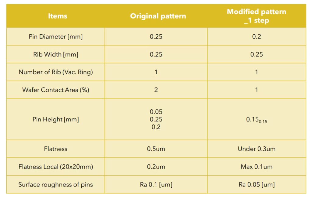
decrease backside particles for sensitive applications, due to lower contact ration (small pin size and wider pitch)
higher edge yield, due to improved edge cell flatness and wider vacuum area
performing durability of the initial flatness and yield improvement, due to superior surface roughness
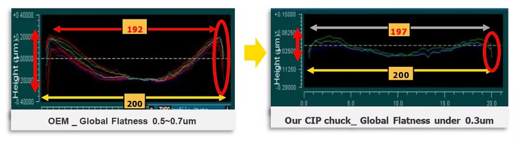
lower overlay value with superior global flatness and wider/stronger vacuum
improve hardness and bending strength, with converting material from Quartz/Si-SiC TO SiC
Technical capabilities OEM vs SPM modified photochuck